Page Not Found
Page not found. Your pixels are in another canvas.

A list of all the posts and pages found on the site. For you robots out there is an XML version available for digesting as well.
Page not found. Your pixels are in another canvas.
About me
This is a page not in th emain menu
This post will show up by default. To disable scheduling of future posts, edit config.yml and set future: false.
This is a sample blog post. Lorem ipsum I can’t remember the rest of lorem ipsum and don’t have an internet connection right now. Testing testing testing this blog post. Blog posts are cool.
This is a sample blog post. Lorem ipsum I can’t remember the rest of lorem ipsum and don’t have an internet connection right now. Testing testing testing this blog post. Blog posts are cool.
This is a sample blog post. Lorem ipsum I can’t remember the rest of lorem ipsum and don’t have an internet connection right now. Testing testing testing this blog post. Blog posts are cool.
This is a sample blog post. Lorem ipsum I can’t remember the rest of lorem ipsum and don’t have an internet connection right now. Testing testing testing this blog post. Blog posts are cool.
Currently offering projects related to GaN systems
I explore material properties and fabrication challenges with wide-bandgaps, such as machining of Silicon Carbide to create high-aspect ratio and 3D structures. Nanofabrication is fun, as pictured! I also look into material properties, such as high field physics of GaAs and GaN, to enable new sensing mechanisms. 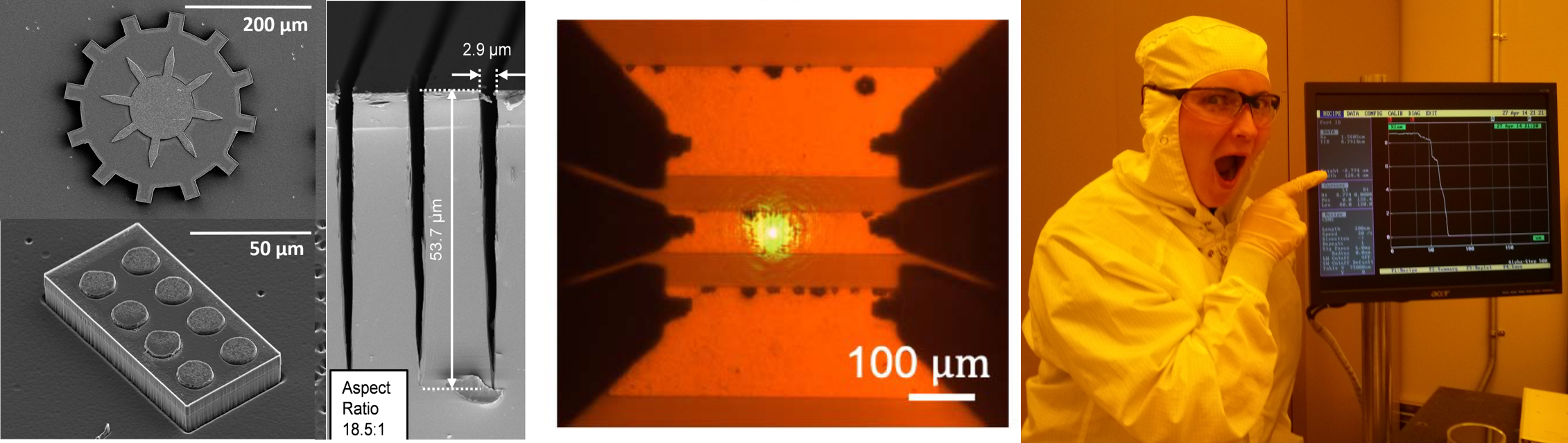
I create novel sensors through new geometries, field engineering, or creative fabrication methods. My main focus is Hall-effect Magnetometers but I also have interest in mechanical sensors (Pressure sensors, accelerometers, etc) 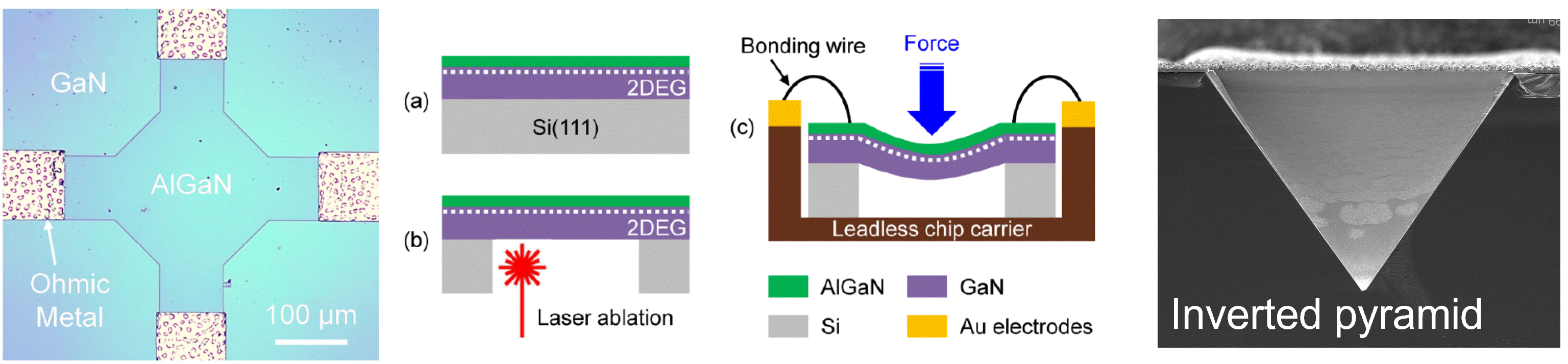
The most exciting element of sensor research is collecting new data in exciting collaborations. In order to do this, we need to create circuits with high-precision readout ability to collect high-quality data. Then we can deploy these devices in interesting environmetns (such as CubeSats, power transformers, and moters) 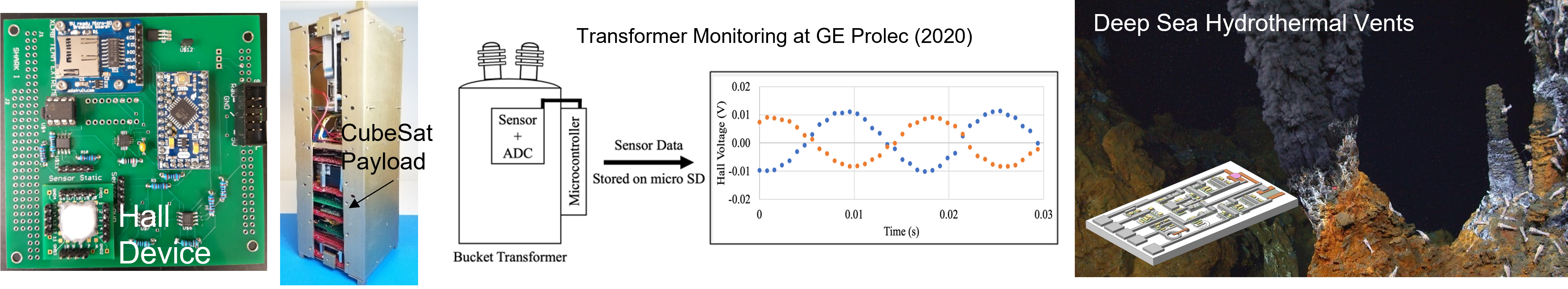
Sadeghi, M.M., Dowling, K., Peterson, R.L., Najafi, K. “High Sensitivity, High Density Micro-Hydraulic Force Sensor Array Using Stereo-Lithography Fabrication Technique,” presented at IEEE MEMS Conference at Taipei, Taiwan. Jan 20-24, 2013, pp 673-676., acceptance rate 40%.
Dowling, K., Suria, A., Shankar, A., Chapin, C., Senesky, D. “Multilayer Etch Masks for 3-Dimensional Fabrication of Robust Silicon Carbide Microstructures,” presented at IEEE MEMS Conference at Estoril, Portugal. Jan 18-22, 2015, pp 284-287., acceptance rate 41%.
Dowling, K., Suria, A., Shankar, A., Lee, H., Won, Y., Asheghi, M., Goodson, K., Senesky, D., “Inductive Coupled Plasma Etching of High Aspect Ratio Silicon Carbide Microchannels for Localized Cooling,” presented at InterpackICNMM2015 at San Francisco, CA July 5-9, 2015. DOI: 10.1115/IPACK2015-48409.
Miller, R., Chapin, C., Dowling, K., Chen, R., Suria, A., Senesky, D., “Low-Temperature Operation of Gallium Nitride Based Ultraviolet Photodetectors,” presented at AIAA SPACE Conferences and Exposition at Long Beach, CA. Sept 13-16, 2013. pp 1-6. DOI: 10.2514/6.2016-5497
Dowling, K.M., Ransom, E.H., Senesky, D.G., “Profile Evolution of High Aspect Ratio Silicon Carbide Trenches using Inductive Coupled Plasma Etching”, IEEE Journal of Microelectromechanical Systems, 2017, 26(1), pp. 135-142.
Ransom, E.H, Dowling, K.M., Rocca-Bejar, D., Palko, J., Senesky, D, “High-Throughput pulse laser manufacturing etch process for complex and released structures from bulk 4H-SiC,” presented at IEEE MEMS Conference at Las Vegas, NV USA January 22-26 2017.
Dowling, K.M., So, H., Toor, A., Chapin, C.A., and Senesky, D.G., “Lithography-free microfabrication of AlGaN/GaN 2DEG strain sensors using laser ablation and direct wirebonding,” Microelectronic Engineering, vol. 173, pp54-57, 2017
Chapin, C., Miller, R., Chen, R., Dowling, K., and Senesky, D., “Low Temperature and Pressure Response of INAlN/GAN Ring-Shaped High Electron Mobility Transistors,” In Proceedings of IEEE Transducers Conference in Kaohsuing, Taiwan, June 18-22,2017.
Chapin, C. A., Miller, R. A., Chen, R., Dowling, K. M., and Senesky, D.G., “InAlN/GaN high electron mobility micro-pressure sensors for high-temperature environments,” Sensors and Actuators A: Physical, Vol. 263, pp. 216–223, 2017.
Yang, M.X., Dowling, K., Senesky, D., and Wong, H.-S.P., “Rapid Prototyping Tape Stencils for the Application of Solder Paste,” presented at the International Symposium on Microelectronics: Fall 2017, Vol. 2017, 1, pp. 000652-00065.
Miller, R. A., So, H., Chiamori, H. C., Dowling, K. M., Wang, Y., and Senesky, D.G., “Graphene-enhanced gallium nitride ultraviolet photodetectors under 2 MeV proton irradiation,” Applied Physics Letters, vol. 111, no. 24, 241902, 2017
Yalamarthy, A.S., Miller, R.A., Dowling, K.M., and Senesky, D.G., “Piezoelectric 2DEG "Metal" Electrodes for High Responsivity, Low Dark Current AlGaN/GaN Photodetectors,” In Proceedings of Compound Semiconductor Week (CSW), Boston, MA, 2018.
Dowling, K.M., Alpert, H.S., Zhang, P., Ramirez, A.N., Yalamarthy, A.S., Köck, H., Ausserlechner, U., and Senesky, D.G. , “The Effect of Bias Conditions on AlGaN/GaN 2DEG Hall Plates,” In Proceedings of Solid-State Sensors, Actuators and Microsystems Workshop, Hilton Head, SC, 2018
Chapin, C.A., Dowling, K.M., Phan, H.P., Chen, R., and Senesky, D.G. ,“Temperature-Dependent Transient Behavior of AlGaN/GaN High Electron Mobility Pressure Sensors,” In Proceedings of Solid-State Sensors, Actuators and Microsystems Workshop, Hilton Head, SC, 2018.
Phan, H.-P., Dowling, K.M., Ngyuen, T.-K., Dinh, T., Senesky, D.G., Namazu, T., Dao, D.V., and Nguyen, N.-T., “Highly sensitive pressure sensors employing 3C-SiC nanowires fabricated on a free standing structure,” Materials & Design, vol. 156, pp. 16-21, 2018
Ngyuyn, T.K., Phan, H.-P,, Dinh, T., Dowling, K.M., Foisal, A.R., Senesky, D.G., Nguyen, N.-T, and Dao, D.V., “Highly sensitive 4H-SiC pressure sensor at cryogenic and elevated temperatures,” Materials & Design, vol. 156, pp 441-445, 2018.
Phan, H.-P., Dowling, K.M., Ngyuen, T.-K., Chapin, C.A., Dinh, T., Miller, R.A., Han, J., Iacopi, A., Senesky, D.G., and Nguyen, N.-T., “Characterization of the piezoresistance in highly doped p-type 3C-SiC at cryogenic temperatures,” RSC Advances, vol. 8, pp. 29976-29979, 2018.
Alpert, H.S., Dowling, K.M., Chapin, C.A., Yalamarthy, A.S., Benbrook, S.R., Köck, H., Ausserlechner, U., and Senesky, D.G., “Effect of Geometry on Sensitivity and Offset of AlGaN/GaN and InAlN/GaN Hall-effect Sensors,” IEEE Sensors Journal, Vol. 19, 10, pp 3640-3646, 2019.
Dowling, K.M., Alpert, H.S., Yalamarthy, A.S., Satterthwaite, P.F., Kumar, S., Köck, H., Ausserlechner, U., and Senesky, D.G., “Micro-Tesla Offset in Thermally Stable AlGaN/GaN 2DEG Hall-effect Plates using Current Spinning,” IEEE Sensors Letters, Vol 3. 3, 2019.
Yalamarthy, A.S., Muñoz Rojo, M., Bruefach, A., Boone, D., Dowling, K.M., Satterthwaite, P.F., Goldhaber-Gordon, D., Pop, E. and Senesky, D.G., “Significant Phonon Drag Enables High Power Factor in the AlGaN/GaN Two-Dimensional Electron Gas,” Nano letters. 2019.
Nguyen, T.-K., Phan, H.-P., Dowling, K.M., Yalamarthy, A.S., Dinh, T., Balakrishnan, V., Liu, T., Chapin, C.A., Truong, Q.-D., Dau, V.T., Goodson, K.E., Senesky, D.G., Dao, D.V., Nguyen, N-T., Lithography and Etching-Free Microfabrication of Silicon Carbide on Insulator Using Direct UV Laser Ablation, Advanced Engineering Materials, vol. 22, 4, p. 1901173, 2020.
Alpert, H.S., Chapin, C.A., Dowling, K.M., Benbrook, S.R., Köck, H., Ausserlechner, U., Senesky, D.G., “Sensitivity of 2DEG-based Hall-effect sensors at high temperatures,” Review of Scientific Instruments, vol. 91, 2, p 025003, 2020.
Dowling, K.M., Liu, T., Alpert, H.S., Chapin, C.A., Eisner, S.R., Yalamarthy, A., Satterthwaite, P.F., Köck, H., Ausserlechner, U., Asheghi, M., Goodson, K.E., and Senesky, D.G., “Low Offset and Noise in High Biased GaN 2DEG Hall-Effect Plates Investigated with Infrared Microscopy,” Journal of Microelectromechanical Systems, vol. 29, 5, pp.1-8, 2020.
Janowitz, J., Holliday, M., Dowling, K., Yeung, B., Kumar, S., Peterson, R., Alpert, H., Chapin, C., Lopez, J., and Senesky, D.G. , “Deployment of InAlN/GaN Hall-effect Sensors for Bucket Transformer Monitoring and Forecasting,” In Proceedings of IEEE Sensors, Virtual Conference, 2020.
Rakheja, S. Li, K., Dowling, K.M., Conway, A.M, and Voss, L.F., “Design and simulation of near-terahertz GaN photoconductive switches- operation in the negative differential mobility regime and pulse compression,” IEEE Journal of Electron Devices Society, vol. 9, pp. 521-532, 2021.
Milestone, W., Guo, D., Sanati, M., Dowling, K.M., Hau-Riege, S., Voss, L.F., Conway, A., and Joshi, R.P., “Monte Carlo transport analysis to assess intensity dependent response of a carbon-doped GaN photoconductor,” Journal of Applied Physics, vol. 129, 19, p. 195703, 2021.
Mukherjee, S., Dowling, K.M., Dong. Y, Li, K. Conway, A., Rakheja, S., and Voss, L., “A Prony-based curve-fitting method for characterization of RF pulses from optoelectronic devices,” IEEE Signal Processing Letters, vol. 29, pp. 364-368, 2021.
Dowling, K.M., Dong, Y., Hall, D., Mukherjee, S., Schneider, J.D., Hau-Riege, S., Harrison, S.E., Leos, L., Conway, A., Rakheja, S., and Voss, L.F., “Pulse Compression Photoconductive Switching Using Negative Differential Mobility,” IEEE Transactions on Electron Devices, vol. 69, 2, pp. 590-596, 2022.
Dong, Y., Dowling, K.M., Hau-Riege, S., Conway, A., Voss, L.F., and Rakheja, S., “Design considerations for gallium arsenide pulse compression photoconductive switch,” Journal of Applied Physics, vol. 131, 13, pp. 134504, 2022.
Mazumder,S.K., Voss, L.F., Dowling, K.M., Conway,A., Hall, D., Kaplar, R.J., Pickrell, G.W., Flicker, J., Binder, A.T., Chowdhury, S., Veliadis,V. Luo, F., Khalil, S., Aichinger,T., Bahl,S.R., Meneghini, M., and Charles, A.B., “Overview of wide/ultrawide bandgap power semiconductor devices for distributed energy resources,” IEEE Journal of Emerging and Selected Topics in Power Electronics , vol. 11, no. 4, pp. 3957 - 3982, 2023.
Dong, Y., Dowling, K.M., Ghandiparsi, S., Voss, L.F., and Rakheja, S., “Observation and Modeling of Near-Bistable Dark-Mode Current-Voltage Characteristics in Semi-Insulating Gallium Arsenide With Implications for Photoconductors,” IEEE Journal of the Electron Devices Society, vol. 11, pp. 385 - 398, 2023.
Ruggeri. J., Strube. J., Dowling, K.M., “3D Hall-Effect Magnetometer Using a Single Inverted Pyramid Structure,” 2024 IEEE 37th International Conference on Micro Electro Mechanical Systems (MEMS), 2024.
Dowling, K.M., Chatterjee, B., Ghandiparsi, S., Shao, Q., Varley, J., Schneider, J.D., Chapin,C., Gottlieb, M.S., Leos, L., Sword, M., Harrsion, S., and Voss, L.F. “Evaluation of Fe-βGa2O3 for Photoconductive Semiconductor Switching,” IEEE Transactions on Electron Devices, vol. 71, no. 3, pp. 1535 - 1540, 2024.
Ruggeri. J., Ausserlechner. U.,Koeck, H., Dowling, K.M., “Inverted pyramid 3-axis silicon Hall-effect magnetic sensor with offset cancellation,” Microsyst Nanoeng, vol. 11, no. 26, 2025.
Gradaute Level Course, Stanford University, Department of Electrical Engineering, 2018
I was the first teaching assistant for Prof. Jim Plummer’s new power devices course on wide-bandgap devices, EE218 at Stanford. I assistend in course material development and provided extra guidance at office hours and lecture tutorials.
Undegraduate Course, TU Delft, Electrical Engineering, 2022
I am currently one of the faculty tutors for EE1L11: the Booming Bass project class.
We welcome Jannik as our first PhD candidate!